Understanding PCB Design: A Comprehensive Guide
15 يناير 2025Sarah Chen, Senior Creative Technologist4 min read

Printed Circuit Boards (PCBs) are the foundation of every electronic device, from smartphones to industrial equipment. Whether you're a startup developing your first hardware product or an engineer optimizing designs, understanding PCB design fundamentals is crucial for success.
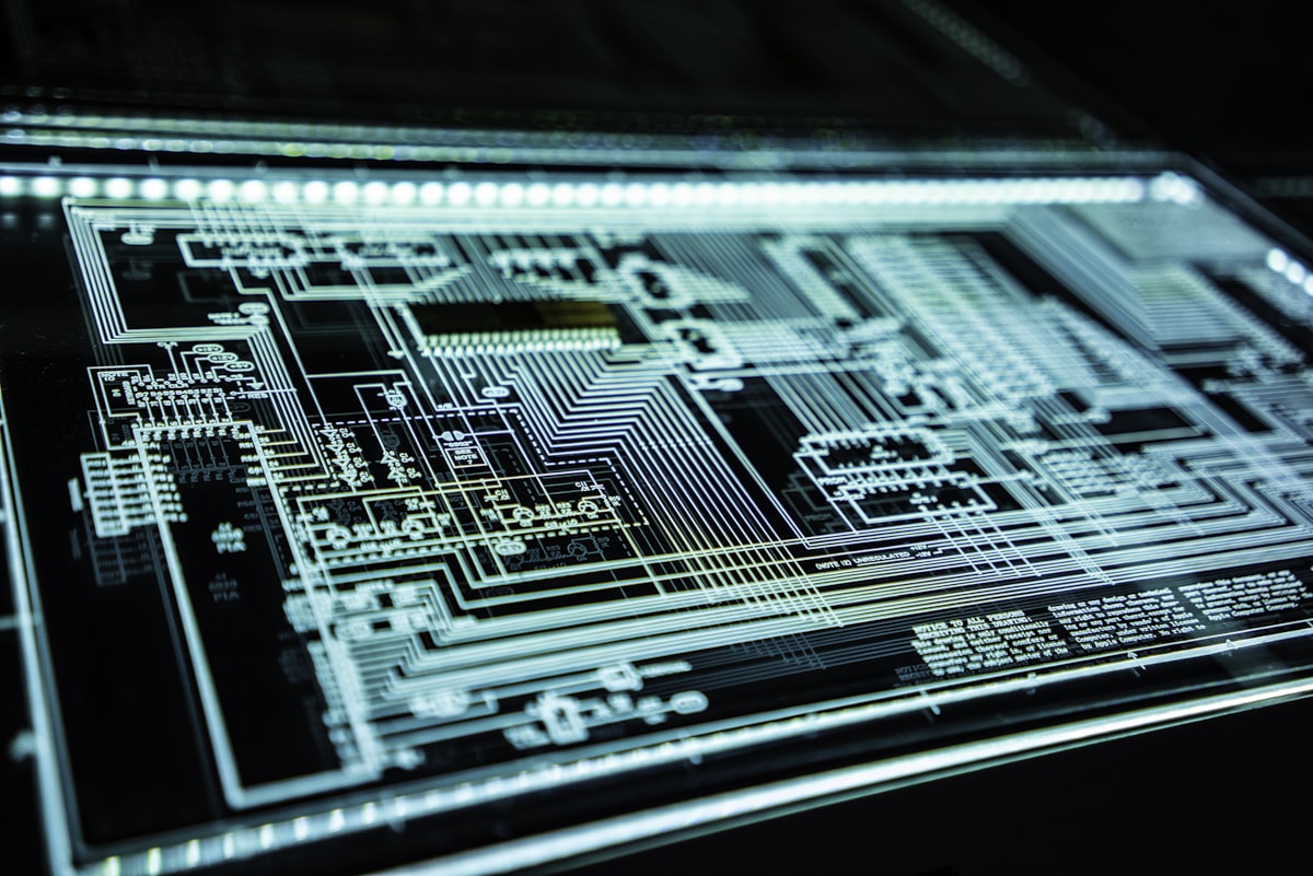
Understanding Schematic Design
The journey begins with schematic capture - translating your circuit idea into a standardized diagram. Modern tools like KiCad, Altium Designer, and Eagle make this process intuitive, but understanding the principles is key:
- Component symbols: Learn standard symbols for resistors, capacitors, ICs, and connectors
- Net naming: Use clear, hierarchical naming (VCC_3V3, GND_ANALOG, SPI_MOSI)
- Design blocks: Organize your schematic into functional blocks (power supply, MCU, sensors)
- Annotation: Add voltage levels, critical frequencies, and design notes

Strategic Component Selection
Component selection impacts cost, availability, and manufacturability. Our experience manufacturing across three continents has taught us these critical factors:
Availability and Lead Times
- Prioritize components with multiple suppliers and stable availability
- Check distributor stock levels and manufacturer lifecycle status
- Consider geographic availability - some parts are region-specific
- Plan for 15-20% component cost fluctuation in your budget
Package Selection
Choose packages that balance size, thermal performance, and assembly complexity:
- 0603/0402 passives: Standard for most designs, good availability
- QFN/DFN packages: Excellent thermal performance, smaller footprint
- BGA packages: High pin count but requires X-ray inspection
- Through-hole: Use sparingly for connectors and high-stress components
PCB Layout Best Practices
Layout transforms your schematic into a physical design. This phase determines signal integrity, thermal performance, and manufacturability:
Layer Stack-up Planning
Start with the right layer configuration:
- 2-layer: Simple designs, cost-effective, limited routing
- 4-layer: Better EMI performance, dedicated power/ground planes
- 6+ layers: High-speed designs, impedance control, dense routing
Routing Guidelines
- Keep high-speed differential pairs matched within 5 mils
- Maintain 3W spacing between traces (3x trace width) for crosstalk reduction
- Use 45° angles instead of 90° for better signal integrity
- Place decoupling capacitors within 0.5" of IC power pins
Design for Manufacturing (DFM)
Great designs consider manufacturing from day one. Here's what our production team checks:
Manufacturing Tolerances
- Minimum trace width: 0.15mm (6 mil) for standard, 0.1mm (4 mil) for advanced
- Via size: 0.3mm (12 mil) minimum, 0.2mm (8 mil) for HDI
- Solder mask clearance: 0.05mm minimum from pad edge
- Silkscreen: 0.15mm line width, 1mm character height
Assembly Considerations
- Maintain 0.25mm courtyard between components
- Use fiducial markers for automated optical inspection
- Panelize boards for efficient assembly (consider V-scoring vs tab-routing)
- Add testpoints for in-circuit testing (ICT) on critical nets
Cost Optimization Strategies
Smart design decisions can significantly reduce manufacturing costs:
- Standard materials: FR-4 with 1oz copper is most economical
- Minimize layer count: Each additional layer adds 20-30% cost
- Standard finishes: HASL is cheapest, ENIG for better shelf life
- Consolidate part count: Use resistor arrays and multi-channel ICs
Common Pitfalls to Avoid
Learn from these frequent issues we see in design reviews:
- Insufficient thermal relief: Large copper pours need thermal reliefs for soldering
- Missing test points: Add them early, removing them later is easy
- Inadequate power delivery: Calculate current paths and use appropriate trace widths
- Poor connector placement: Consider cable routing and mechanical stress
- Forgotten mounting holes: Plan mechanical integration from the start
Next Steps
Ready to move from design to production? Our team can review your design for manufacturability, suggest cost optimizations, and guide you through prototyping and mass production. With facilities in Shenzhen, we offer rapid prototyping with 24-hour turns and seamless scaling to volume production.
Contact our engineering team at rfq@source.parts for a manufacturing quote and consultation.
مقالات ذات صلة

ManufacturingPrototyping
From Prototype to Mass Production: Scaling Your Hardware Product
Learn the key stages and considerations when taking your electronic hardware from a single prototype to mass production.
اقرأ المزيد
MCUMicrocontroller
Choosing the Right Microcontroller for Your Project
A guide to selecting the perfect microcontroller (MCU) based on your project's requirements, considering factors like processing power, peripherals, and cost.
اقرأ المزيد
EMCCompliance
Navigating EMC Compliance for Electronic Devices
Understanding Electromagnetic Compatibility (EMC) is crucial for bringing electronic products to market. Learn about testing and design best practices.
اقرأ المزيد